- 您现在的位置:买卖IC网 > Sheet目录3832 > AT87C52X2-3CSUM (Atmel)IC 8051 MCU 8K OTP 40MHZ 40DIP
34
TS8xCx2X2
4184I–8051–02/08
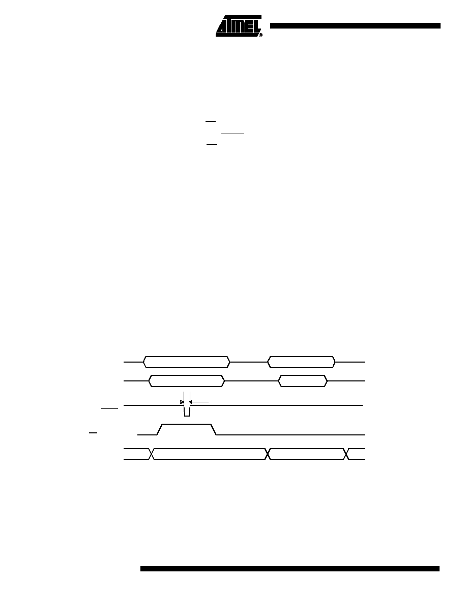
Programming Algorithm
The Improved Quick Pulse algorithm is based on the Quick Pulse algorithm and
decreases the number of pulses applied during byte programming from 25 to 1.
To program the TS87C52X2 the following sequence must be exercised:
Step 1: Activate the combination of control signals.
Step 2: Input the valid address on the address lines.
Step 3: Input the appropriate data on the data lines.
Step 4: Raise EA/VPP from VCC to VPP (typical 12.75V).
Step 5: Pulse ALE/PROG once.
Step 6: Lower EA/VPP from VPP to VCC
Repeat step 2 through 6 changing the address and data for the entire array or until the
end of the object file is reached (See Figure 12.).
Verify Algorithm
Code array verify must be done after each byte or block of bytes is programmed. In
either case, a complete verify of the programmed array will ensure reliable programming
of the TS87C52X2.
P 2.7 is used to enable data output.
To verify the TS87C52X2 code the following sequence must be exercised:
Step 1: Activate the combination of program and control signals.
Step 2: Input the valid address on the address lines.
Step 3: Read data on the data lines.
Repeat step 2 through 3 changing the address for the entire array verification (See Fig-
The encryption array cannot be directly verified. Verification of the encryption array is
done by observing that the code array is well encrypted.
Figure 12. Programming and Verification Signal’s Waveform
EPROM Erasure
(Windowed Packages
Only)
Erasing the EPROM erases the code array, the encryption array and the lock bits return-
ing the parts to full functionality.
Erasure leaves all the EPROM cells in a 1’s state (FF).
Erasure Characteristics
The recommended erasure procedure is exposure to ultraviolet light (at 2537 ) to an
integrated dose at least 15 W-sec/cm2. Exposing the EPROM to an ultraviolet lamp of
Control signals
Data In
ALE/PROG
A0-A12
Programming Cycle
100s
D0-D7
EA/VPP
Data Out
Read/Verify Cycle
12.75V
5V
0V
发布紧急采购,3分钟左右您将得到回复。
相关PDF资料
PIC16C924-04/L
IC MCU OTP 4KX14 LCD DVR 68PLCC
PIC16F767-I/SO
IC PIC MCU FLASH 8KX14 28SOIC
PIC24FJ64GA310-I/PF
MCU 16BIT 64KB FLASH 100TQFP
DSPIC33FJ64GP202-E/MM
IC DSPIC MCU/DSP 64K 28-QFN
PIC16F876A-I/ML
IC MCU FLASH 8KX14 A/D 28QFN
PIC16F876A-I/SO
IC MCU FLASH 8KX14 EE 28SOIC
PIC16F876A-I/SP
IC MCU FLASH 8KX14 EE 28DIP
AT87C51RD2-3CSUM
IC 8051 MCU 64K OTP 40MHZ 40DIP
相关代理商/技术参数
AT87C52X2-3CSUV
功能描述:8位微控制器 -MCU Microcontroller
RoHS:否 制造商:Silicon Labs 核心:8051 处理器系列:C8051F39x 数据总线宽度:8 bit 最大时钟频率:50 MHz 程序存储器大小:16 KB 数据 RAM 大小:1 KB 片上 ADC:Yes 工作电源电压:1.8 V to 3.6 V 工作温度范围:- 40 C to + 105 C 封装 / 箱体:QFN-20 安装风格:SMD/SMT
AT87C52X2-RLRUM
功能描述:8位微控制器 -MCU 0.5um RoHS:否 制造商:Silicon Labs 核心:8051 处理器系列:C8051F39x 数据总线宽度:8 bit 最大时钟频率:50 MHz 程序存储器大小:16 KB 数据 RAM 大小:1 KB 片上 ADC:Yes 工作电源电压:1.8 V to 3.6 V 工作温度范围:- 40 C to + 105 C 封装 / 箱体:QFN-20 安装风格:SMD/SMT
AT87C52X2-RLTUL
功能描述:8位微控制器 -MCU C72X2C52 0.5m OTP RoHS:否 制造商:Silicon Labs 核心:8051 处理器系列:C8051F39x 数据总线宽度:8 bit 最大时钟频率:50 MHz 程序存储器大小:16 KB 数据 RAM 大小:1 KB 片上 ADC:Yes 工作电源电压:1.8 V to 3.6 V 工作温度范围:- 40 C to + 105 C 封装 / 箱体:QFN-20 安装风格:SMD/SMT
AT87C52X2-RLTUM
功能描述:8位微控制器 -MCU C72X2 C52 0.5 m X 2 OTP 0.5 NV RoHS:否 制造商:Silicon Labs 核心:8051 处理器系列:C8051F39x 数据总线宽度:8 bit 最大时钟频率:50 MHz 程序存储器大小:16 KB 数据 RAM 大小:1 KB 片上 ADC:Yes 工作电源电压:1.8 V to 3.6 V 工作温度范围:- 40 C to + 105 C 封装 / 箱体:QFN-20 安装风格:SMD/SMT
AT87C52X2-RLTUV
制造商:ATMEL 制造商全称:ATMEL Corporation 功能描述:8-bit Microcontroller 8 Kbytes ROM/OTP, ROMless
AT87C52X2-SLRUL
功能描述:8位微控制器 -MCU Microcontroller RoHS:否 制造商:Silicon Labs 核心:8051 处理器系列:C8051F39x 数据总线宽度:8 bit 最大时钟频率:50 MHz 程序存储器大小:16 KB 数据 RAM 大小:1 KB 片上 ADC:Yes 工作电源电压:1.8 V to 3.6 V 工作温度范围:- 40 C to + 105 C 封装 / 箱体:QFN-20 安装风格:SMD/SMT
AT87C52X2-SLRUM
功能描述:8位微控制器 -MCU Microcontroller RoHS:否 制造商:Silicon Labs 核心:8051 处理器系列:C8051F39x 数据总线宽度:8 bit 最大时钟频率:50 MHz 程序存储器大小:16 KB 数据 RAM 大小:1 KB 片上 ADC:Yes 工作电源电压:1.8 V to 3.6 V 工作温度范围:- 40 C to + 105 C 封装 / 箱体:QFN-20 安装风格:SMD/SMT
AT87C52X2-SLSUL
功能描述:8位微控制器 -MCU OTP C52/8K 40MHZ 3V COM RoHS:否 制造商:Silicon Labs 核心:8051 处理器系列:C8051F39x 数据总线宽度:8 bit 最大时钟频率:50 MHz 程序存储器大小:16 KB 数据 RAM 大小:1 KB 片上 ADC:Yes 工作电源电压:1.8 V to 3.6 V 工作温度范围:- 40 C to + 105 C 封装 / 箱体:QFN-20 安装风格:SMD/SMT